Aperture Time, Aperture Delay Time, and Aperture Jitter
Perhaps the most misunderstood and misused ADC and sample-and-hold (or track-andhold)
specifications are those that include the word aperture. The most essential dynamic
property of a SHA is its ability to disconnect quickly the hold capacitor from the input
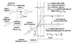
buffer amplifier as shown in Figure 2.77. The short (but non-zero) interval required for
this action is called aperture time (or sampling aperture), ta. The actual value of the
voltage that is held at the end of this interval is a function of both the input signal slew
rate and the errors introduced by the switching operation itself. Figure 2.77 shows what
happens when the hold command is applied with an input signal of two arbitrary slopes
labeled as 1 and 2. For clarity, the sample-to-hold pedestal and switching transients are
ignored. The value that is finally held is a delayed version of the input signal, averaged
over the aperture time of the switch as shown in Figure 2.77. The first-order model
assumes that the final value of the voltage on the hold capacitor is approximately equal to
the average value of the signal applied to the switch over the interval during which the
switch changes from a low to high impedance (ta).
The model shows that the finite time required for the switch to open (ta) is equivalent to
introducing a small delay te in the sampling clock driving the SHA. This delay is constant
and may either be positive or negative. The diagram shows that the same value of te
works for the two signals, even though the slopes are different. This delay is called
???? NF decreases with increasing source resistance.
???? NF decreases with increasing ADC input bandwidth if there is no
input filtering.
???? In both cases, the circuit noise increases, and the NF decreases.
???? The reason NF decreases is that the source noise makes up a
larger component of the total noise (which remains relatively
constant because the ADC noise is much greater than the source
noise).
???? In practice, input filtering is used to limit the input noise bandwidth
and reduce overall system noise.
???? ADCs have relatively high NF compared to other RF parts. In the
system the ADC should be preceded with low-noise gain blocks.
???? Exercise caution when using NF!
FUNDAMENTALS OF SAMPLED DATA SYSTEMS
2.3 DATA CONVERTER AC ERRORS
2.69
effective aperture delay time, aperture delay time, or simply aperture delay, te. In an
ADC, the aperture delay time is referenced to the input of the converter, and the effects of
the analog propagation delay through the input buffer, tda and the digital delay through
the switch driver, tdd, must be considered. Referenced to the ADC inputs, aperture time,
te', is defined as the time difference between the analog propagation delay of the front-end
buffer, tda, and the switch driver digital delay, tdd, plus one-half the aperture time, ta/2.
...
If, however, there is sample-to-sample variation in aperture delay (aperture jitter), then a
corresponding voltage error is produced as shown in Figure 2.79. This sample-to-sample
variation in the instant the switch opens is called aperture uncertainty, or aperture jitter
and is usually measured in rms picoseconds. The amplitude of the associated output error
is related to the rate-of-change of the analog input. For any given value of aperture jitter,
the aperture jitter error increases as the input dv/dt increases. The effects of phase jitter
on the external sampling clock (or the analog input for that matter) produce exactly the
same type of error.


